Medium-grain reconfiguration tutorial
This tutorial shows how to build a medium-grain reconfigurable system. This tutorial uses the same static system created in the previous tutorial. In this case the reconfigurable partition is virtually divided into two regions that are connected directly to each other (without using static system resources). This tutorial builds four different reconfigurable modules. Two reconfigurable modules (add and substract) can be allocated in the top part of the region and the other two reconfigurable modules (shift one bit right and shift two bits right) can be allocated in the bottom part of the reconfigurable region.
Requirements
- Coarse-grain tutorial
- Basic knowledge of Vivado and Xilinx SDK
- The tutorial is implemented in a xc7z020clg400-1 SoC. This tutorial can be followed almost entirely without having the device. The only limitation is that the user cannot test if the system is working correctly.
Implementing the reconfigurable system with IMPRESS
The input files to build the reconfigurable system are located in <path to IMPRESS>/examples/medium_grain/. In this case the project_info file only describes the reconfigurable modules as the static system is reused from the previous tutorial and it is not implemented again. Being a medium-grain reconfigurable system the virtual architecture of the reconfigurable system differs from the virtual architecture used in the static system.
Open Vivado and introduce the following commands:
source <path to IMPRESS>/design_time/reconfiguration_tool/impress.tcl
implement_reconfigurable_design <path to IMPRESS>/examples/medium_grain/project_info
This generates a folder called IMPRESS_build that contains synthesis & implementation checkpoints and the static and partial bitstreams.
Run-time management
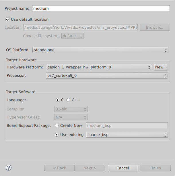
Now we will build the software program in charge of downloading the partial bitstreams. First, open the project where we built the static system sources in the coarse-grain tutorial and open the SDK. Create a new project by clicking File->New->Application Project. Name the project medium and select use existing BSP coarse_bsp (the BSP generated in the previous tutorial), click next and select Empty application.
Now we have to import IMPRESS run_time source files to the SDK project. Import the files xc7z020 (.c and .h) and series7.h from <path to IMPRESS>/run_time/FPGA_templates and files IMPRESS_reconfiguration (.c and .h) and reconfig_pcap (.c and .h) from *
Testing the system
Once the source files have been imported into the project we can test the system in the FPGA.
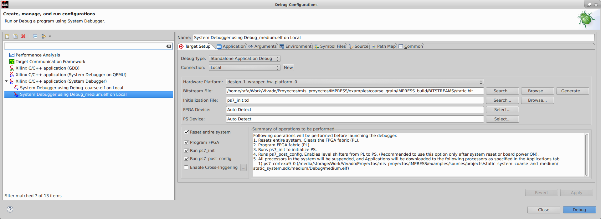
First connect the board (e.g., PYNQ or Zedboard) to the computer. Insert in the board an SD memory card with the partial bitstreams stored in <path to IMPRESS>/examples/medium_grain/impress_build/BITSTREAMS/. Right-click in the project and select debug as->debug configurations select the last option (system debugger). In the bitstream field select browse and select the static bitstream stored in <path to IMPRESS>/examples/coarse_grain/impress_build/BITSTREAMS/static.bit. Check reset entire system and press Debug.
Press Step over or F6 until the SHIFT1 and ADD modules are reconfigured. Now go to to the static system project and select Open Target -> Auto Connect in the flow navigator ribbon.
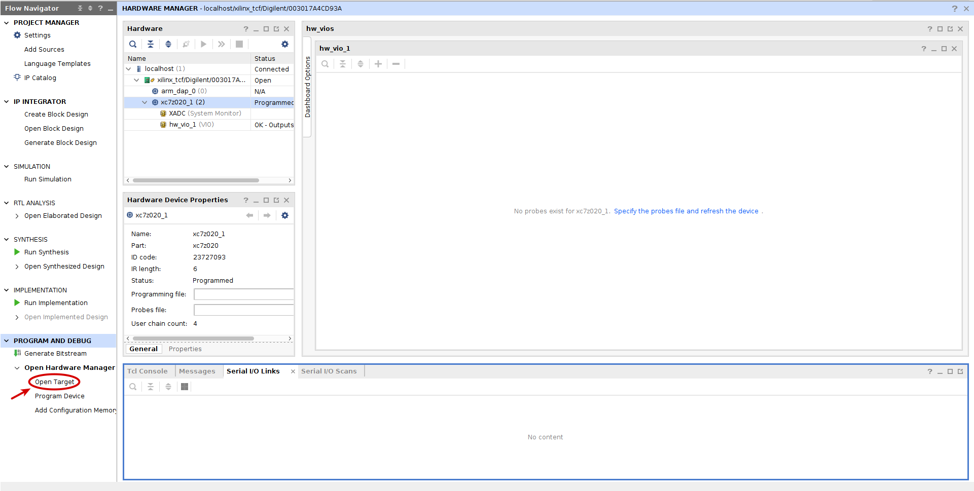
Click the Specify the probes (.ltx) file and refresh the device button and select the probes generated under the static bitstream folder in <path to IMPRESS>/examples/coarse_grain/impress_build/BITSTREAMS/static_probes.ltx Add all the probes and give different values to probes vio_0_probe_out0 and vio_0_probe_out1. vio_0_probe_out2 is the reset signal of the reconfigurable module and its value should be 0. Check that the value of probe reconf_part_0_output1[7:0] is the sum of both values divided by two (add and shift one bit to the right).
NOTE: in this tutorial it is not necessary to reset the module before using it to ensure that the module works correctly but this may be the case in more complex reconfigurable modules.
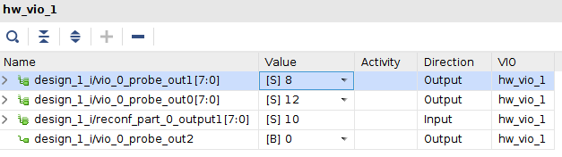
Then, click step over and check that probe reconf_part_0_output1[7:0] value is the sum of both inputs divided by 4 (add and shift two bits to the right). Do it again and check that now the value is the subtraction of both inputs divided by 4 (subtract and shift two bits to the right).